- 您现在的位置:买卖IC网 > Sheet目录401 > CPC3703CTR (IXYS Integrated Circuits Division)MOSFET N-CH 250V 360MA SOT-89
�� �
�
�I� NTEGRATED� C� IRCUITS� D� IVISION�
�Absolute� Maximum� Ratings� @� 25oC� (Unless� Otherwise� Noted)�
�CPC3703�
�Parameter�
�Drain-to-Source� Voltage�
�Gate-to-Source� Voltage�
�Pulsed� Drain� Current�
�Total� Package� Dissipation� 1�
�Junction� Temperature�
�Operational� Temperature,� Ambient�
�Storage� Temperature�
�Ratings�
�250�
�±15�
�600�
�1.1�
�125�
�-55� to� +125�
�-55� to� +125�
�Units�
�V� P�
�V� P�
�mA�
�W�
�o� C�
�o� C�
�o� C�
�Absolute� Maximum� Ratings� are� stress� ratings.� Stresses� in�
�excess� of� these� ratings� can� cause� permanent� damage� to� the�
�device.� Functional� operation� of� the� device� at� conditions� beyond�
�those� indicated� in� the� operational� sections� of� this� data� sheet� is�
�not� implied.�
�1�
�Mounted� on� 1"x1"x0.062"� FR4� board.�
�Electrical� Characteristics� @� 25oC� (Unless� Otherwise� Noted)�
�Parameter�
�Drain-to-Source� Breakdown� Voltage�
�Gate-to-Source� Off� Voltage�
�Change� in� V� GS(off)� with� Temperature�
�Gate� Body� Leakage� Current�
�Drain-to-Source� Leakage� Current�
�Saturated� Drain-to-Source� Current�
�Static� Drain-to-Source� On-State� Resistance�
�Change� in� R� DS(on)� with� Temperature�
�Forward� Transconductance�
�Input� Capacitance�
�Common� Source� Output� Capacitance�
�Reverse� Transfer� Capacitance�
�Turn-On� Delay� Time�
�Rise� Time�
�Turn-Off� Delay� Time�
�Fall� Time�
�Source-Drain� Diode� Voltage� Drop�
�Thermal� Resistance� (Junction� to� Ambient)�
�Symbol�
�V� (BR)DSX�
�V� GS(off)�
�dV� GS(off)� /dT�
�I� GSS�
�I� D(off)�
�I� DSS�
�R� DS(on)�
�dR� DS(on)� /dT�
�G� FS�
�C� ISS�
�C� OSS�
�C� RSS�
�t� d(on)�
�t� r�
�t� d(off)�
�t� f�
�V� SD�
�R� ?� JA�
�Conditions�
�V� GS� =� -5V,� I� D� =100μA�
�V� DS� =� 5V,� I� D� =1mA�
�V� DS� =� 5V,� I� D� =1� ?� A�
�V� GS� =±15V,� V� DS� =0V�
�V� GS� =� -5V,� V� DS� =250V�
�V� GS� =� -5V,� V� DS� =200V,� T� A� =125oC�
�V� GS� =� 0V,� V� DS� =15V�
�V� GS� =� 0V,� I� D� =200mA�
�I� D� =� 100mA,� V� DS� =� 10V�
�V� GS� =� -5V�
�V� DS� =� 25V�
�f=� 1MHz�
�V� DD� =� 25V�
�I� D� =� 150mA�
�V� GS� =� 0V� to� -10V�
�R� gen� =� 50� ?�
�V� GS� =� -5V,� I� SD� =150mA�
�-�
�Min�
�250�
�-1.6�
�-�
�-�
�-�
�-�
�360�
�-�
�-�
�225�
�-�
�-�
�-�
�-�
�Typ�
�-�
�-�
�-�
�-�
�-�
�-�
�-�
�-�
�-�
�-�
�327�
�51�
�27�
�23�
�8�
�17�
�70�
�0.6�
�90�
�Max�
�-�
�-3.9�
�4.5�
�100�
�1�
�1�
�-�
�4�
�1.1�
�-�
�350�
�65�
�35�
�35�
�20�
�25�
�80�
�1.8�
�-�
�Units�
�V�
�V�
�mV/� o� C�
�nA�
�μA�
�mA�
�mA�
�?�
�%/� o� C�
�m�
�pF�
�ns�
�V�
�oC/W�
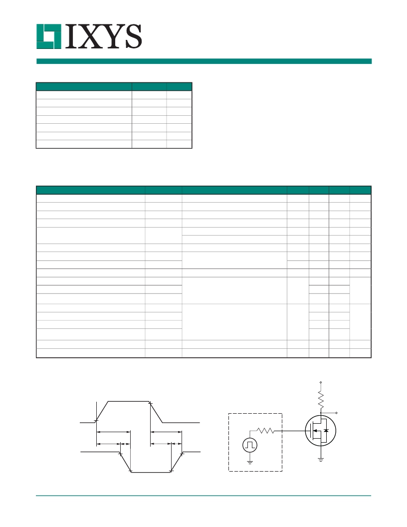
�Switching� Waveform� &� Test� Circuit�
�0V�
�90%�
�PULSE�
�V� DD�
�R� L�
�INPUT�
�GENERATOR�
�OUTPUT�
�-10V�
�10%�
�t� on�
�t� off�
�R� gen�
�V� DS�
�t� d(on)�
�90%�
�tf�
�t� d(off)�
�tr�
�90%�
�INPUT�
�D.U.T.�
�OUTPUT�
�0V�
�10%�
�10%�
�2�
�www.ixysic.com�
�R06�
�发布紧急采购,3分钟左右您将得到回复。
相关PDF资料
CPC5602C
MOSFET N-CH 350V 5MA SOT-223
CPC5603C
MOSFET N-CH 415V 5MA SOT-223
CPDETLS-4000
RF POWER DETECTOR IN-LINE SMA
CPH3348-TL-E
MOSFET P-CH 12V 3A CPH3
CPH3350-TL-H
MOSFET P-CH 20V 3A CPH3
CPH3351-TL-H
MOSFET P-CH 60V 1.8A CPH3
CPH3356-TL-H
MOSFET P-CH 20V 2.5A CPH3
CPH3360-TL-H
MOSFET P-CH 30V 1.6A CPH3
相关代理商/技术参数
CPC3703ZTR
功能描述:MOSFET N-CH 250V SOT-89 制造商:ixys integrated circuits division 系列:- 包装:带卷(TR) 零件状态:有效 FET 类型:MOSFET N 通道,金属氧化物 FET 功能:耗尽模式 漏源极电压(Vdss):250V 电流 - 连续漏极(Id)(25°C 时):- 不同?Id,Vgs 时的?Rds On(最大值):4 欧姆 @ 200mA,0V 不同 Id 时的 Vgs(th)(最大值):- 不同 Vgs 时的栅极电荷(Qg):- 不同 Vds 时的输入电容(Ciss):350pF @ 25V 功率 - 最大值:1.1W 工作温度:-55°C ~ 125°C(TJ) 安装类型:表面贴装 封装/外壳:TO-243AA 供应商器件封装:SOT-89 标准包装:1,000
CPC3708ACTR
制造商:IXYS Integrated Circuits Division 功能描述:CPC
CPC3708CTR
功能描述:MOSFET N-CH 350V 0.005A SOT-89 制造商:ixys integrated circuits division 系列:- 包装:剪切带(CT) 零件状态:停产 FET 类型:MOSFET N 通道,金属氧化物 FET 功能:耗尽模式 漏源极电压(Vdss):350V 电流 - 连续漏极(Id)(25°C 时):5mA(Ta) 不同?Id,Vgs 时的?Rds On(最大值):14 欧姆 @ 50mA,350mV 不同 Id 时的 Vgs(th)(最大值):- 不同 Vgs 时的栅极电荷(Qg):- 不同 Vds 时的输入电容(Ciss):300pF @ 0V 功率 - 最大值:1.1W 工作温度:-40°C ~ 110°C(TA) 安装类型:表面贴装 封装/外壳:TO-243AA 供应商器件封装:SOT-89 标准包装:1
CPC3708ZTR
制造商:IXYS Integrated Circuits Division 功能描述:N-CHANNEL DEPLETION MOSFET 350 V 14 OHMS SOT-223
CPC3710
制造商:CLARE 制造商全称:Clare, Inc. 功能描述:N-Channel Depletion-Mode FET
CPC3710C
功能描述:MOSFET N Channel Depletion Mode FET, 250V SOT-89 RoHS:否 制造商:STMicroelectronics 晶体管极性:N-Channel 汲极/源极击穿电压:650 V 闸/源击穿电压:25 V 漏极连续电流:130 A 电阻汲极/源极 RDS(导通):0.014 Ohms 配置:Single 最大工作温度: 安装风格:Through Hole 封装 / 箱体:Max247 封装:Tube
CPC3710CTR
功能描述:MOSFET N Channel Depletion Mode FET, T/R, 250V SOT-89 RoHS:否 制造商:STMicroelectronics 晶体管极性:N-Channel 汲极/源极击穿电压:650 V 闸/源击穿电压:25 V 漏极连续电流:130 A 电阻汲极/源极 RDS(导通):0.014 Ohms 配置:Single 最大工作温度: 安装风格:Through Hole 封装 / 箱体:Max247 封装:Tube
CPC3714
制造商:CLARE 制造商全称:Clare, Inc. 功能描述:N-Channel Depletion-Mode FET